Carnegie Mellon University
—
—
—
Search
Search
Search this site only
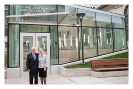
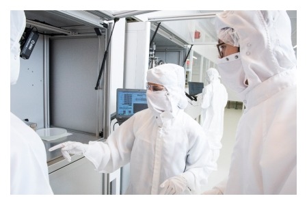
Claire & John Bertucci Nanotechnology Laboratory
College of Engineering
About
Getting Access
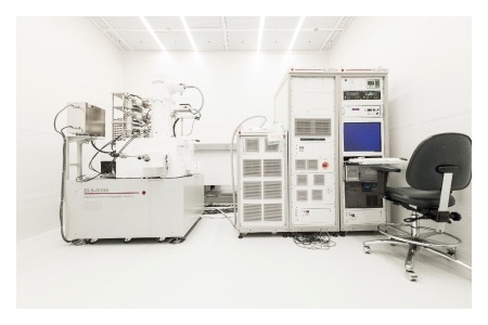
Equipment
Events
May 22 -
May 22
Nanofabrication Futures Symposium
Quick links
Facility Online Manager (FOM) - Internal Access Only